REATISS Unlock patent value
Labs
 Material and Process Analysis Lab
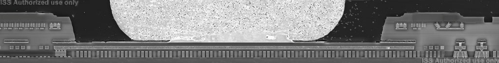
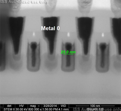
REATISS Material and Process Analysis Lab capabilities allow analyze structure and elemental composition of integrated circuits by means of SEM investigation and EDX spectroscopy analysis. Lab state-of-the-art equipment enables performance of a full cycle of preparation and investigation of semiconductor samples.
Expertise in deposition of different materials as well as modern tools allow preparing samples for high-resolution SEM imaging. Technics and methods are well set and provide excellent repeatability.
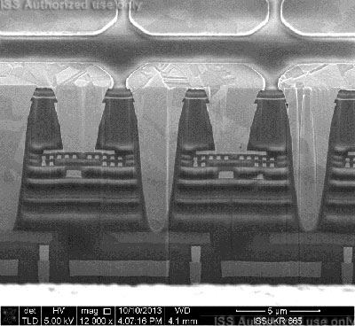
Dual Beam system allows Focused Ion Beam usage with visual SEM control of sample preparation. Skilled FIB operators prepare high quality thin lamellas for STEM high-resolution imaging and EDX analysis.
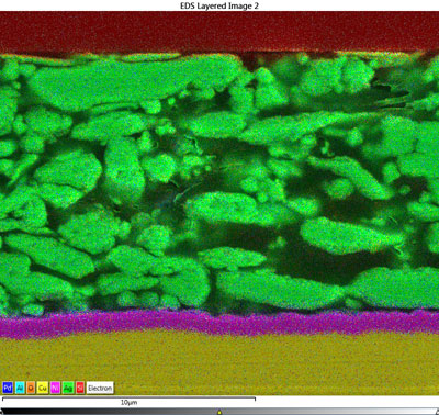
Modern large area silicon drift detector of EDX system allows experts to perform fast and reliable elements recognition. Fast EDX system gives possibility of EDX mapping acquisition. EDX maps give demonstrative and convenient elements distribution picture on the whole image.