REATISS Unlock patent value
Services
 Circuitry Analysis
REATISS provides circuit analysis of semiconductor devices revealing layout and circuit design details. Hierarchically organized reports give client insights into competitive device schematics and uncover evidences of patents infringements. Analysis of competitor circuits could improve design efficiency and reduce design costs.
REATISS circuitry analysis (CE) methodology allows facilitate reverse engineering process and effectively use laboratory capabilities for projects of different complexity. CE project steps:
- Upon receiving samples, First Look Analysis (FLA) is done, including package optical and x-ray images, die top metal level, and die markings images. Results are presented in a form of PDF report.
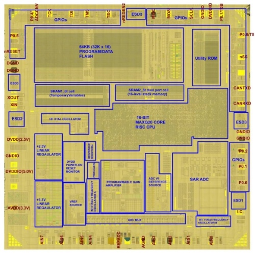
- Next step is Die Architecture and Functional Analysis (AFA). It comprises high-resolution imaging of the die on devices level, analysis of the available documentation and board, identification of IP blocks functionality and preliminary process analysis (number of metals and minimal gate sizes). Results are delivered in a form of PDF report and optional is online access to high-resolution images database.
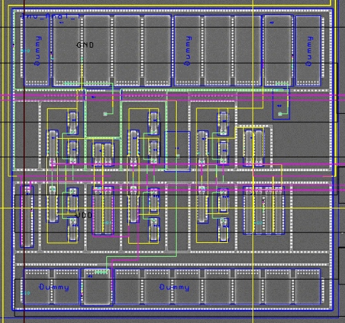
- Following AFA, areas for de-processing and imaging are selected in respect to customer’s interests or targeted patents. Advanced and precise delayering of the die, high-resolution optical and SEM imaging, sophisticated image processing techniques allow to create multi-layer images database for technologies down to 3nm. Results are delivered as online access to high-resolution multi-layer images database.
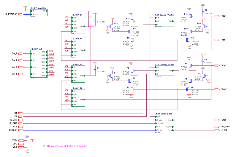
- Multi-layer images database and in-house developed software tools are used to perform layout annotation, devices extraction, and schematic organization into functional hierarchical blocks. Results are delivered in a form of PDF report containing fully analyzed and hierarchically organized schematics.
CE report comprises hierarchically organized schematics of blocks ordered by a customer and device related information such as:
- Device functionality description
- Part identification info (package type, optical and x-ray images of the package, available logical board images)
- Die identification info (process estimation, die markings images, die images on top metal and diffusion layers, die architecture overview, layout images of extracted blocks)
REATISS has successful experience in focused CE projects, where the die areas for extraction are defined according to customer request or a set of suspected patents infringements. This approach helps to reduce project costs and time needed for circuitry analysis.
For each device CE project timeframe is defined separately and highly depends on technology, die area, and number of blocks to be extracted.
Typical cycle time is 3-4 months. Typical CE report could be found here:
Circuitry Report Example